
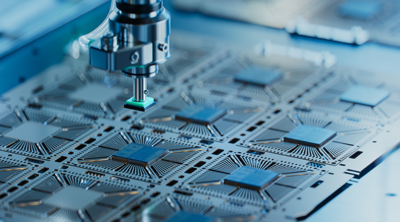

Semiconductor devices such as diodes, transistors and integrated circuits are at the heart of modern-day electronic devices such as smartphones, sensors, computers, medical devices, renewable energy and both automotive and defence technologies.
More recent applications of semiconductors include AI chips, IoT devices such as smart thermostats and 5G communication systems.
What are semiconductors made of and how do they work?
Semiconductors work by controlling the flow of electricity, known as electrical conductivity through a device or circuit. The basis of semiconductors lies in extremely high purity semi-metals such as silicon, gallium or germanium. Typically, silicon is the most frequently chosen semi-metal due to its significantly higher abundance than gallium or germanium (it is the second most common element on earth), its cost-effectiveness, its versatility and its relative ease of handling.
Silicon also has a band-gap (i.e. the energy difference between the valence and conduction bands) that allow for precise control of the flow of electrical currents. This is essential for applications in digital and signal processing. Silicon can also form a stable, extremely thin oxide layer on its surface that render it suitable for high temperature applications.
Silicon doping and its effect on conductivity
The addition of very carefully controlled, very low quantities quantities of similarly high purity selected materials known as dopants into the semi-metal crystal lattice allows the conductivity to be modified in a very controlled manner. Typically, the dopant concentration is just 1 part dopant to 100 million parts of semi-metal in low- or lightly-doped semiconductors, whilst in highly- or heavily-doped semiconductors, the dopant concentration can be of the order of one part dopant to 10,000 parts of semi-metal.
The addition of phosphorus or arsenic dopants to silicon, for example, gives a crystal lattice in which the dopant replaces some of the silicon atoms giving an n-type semiconductor that shows increased conductivity compared to un-doped silicon due to the presence of an extra electron (the charge carrier) in the dopant that makes electron flow through the crystal lattice much easier.
On the other hand, the replacement of some of the silicon atoms in the crystal lattice by a dopant such as boron, aluminium, gallium or indium gives rise to an electron deficiency known as a “hole” that behaves like a mobile positive charge carrier that also leads to an increase in conductivity. These are known as p-type semiconductors. Doping has to be carried out under very precise conditions to control the concentration and regions of p- and n-type dopants. By connecting a p-type semiconductor to an n-type semiconductor in a single crystal, a device known as a p-n junction is obtained. One single crystal can contain many p-n junctions. These devices allow electrical current to flow through them only in one direction.
What effects does impurities have on semiconductor performance?
Because small amount of impurities can have a significant effect on the extent to which current flows through a semiconductor, the presence of unwanted impurities can have a disastrous effect on the performance and reliability of the semiconductor. Even a dust particle invisible to the naked eye can render an entire batch of semiconductor defective resulting in expensive losses of an entire batch, primarily because the defects are not detected until late-stage testing is performed.
Other airborne contaminants that interfere with the precise manufacturing processes can include skin cells, bacteria, chemical vapours, particles emitted from machinery, contaminants from outside of the cleanroom and fluctuations in humidity.
Reducing the risk of contamination and improving reliability
To reduce the risk of contamination, semiconductor manufacture is carried out in sterile cleanrooms in which the air quality and the presence of particulates and impurities in fluids used in the manufacturing process is tightly controlled. Air quality is controlled by a number of systems in the cleanroom such as High Efficiency Particulate Air (HEPA) and Ultra-Low Penetration Air (ULPA) filters which remove 99.99% of airborne contaminants, but the use of laminar airflow systems, positive air pressure and airborne chemical filtration all contribute to a significant reduction in contaminant concentration, whilst control of humidity levels prevents static discharge and oxidation.
Control of the temperature in the cleanroom helps to give a consistent finished product because semiconductors show increasing conductivity at higher temperatures.
Why 0.2 Micron Filtration is critical
Fluids, such as ultrapure water, are used for polishing semiconductor wafers and for ensuring the cleanliness of the processing facility, whilst developers and peeling aids are used to remove photoresistive and other materials during the manufacturing process.
Suspended solids and/or bacteria in all of these fluids have the potential to contaminate the semiconductor. Typically, bacteria have a size range of 0.2 – 5µm in size and so removal of these impurities is carried out by filtering the fluids using a filter with a pore size of 0.2µm PFTE or PES filter. These materials are used because they offer exceptional chemical resistance, low particle loss and compatibility even with the most aggressive of solvents where the small pore size of the filter permits even the smallest of bacteria, such as those belonging to the genus Mycoplasma, can be readily removed from the fluid.
A combination of all of the above purification methods have significantly improved the reproducibility and reliability of semiconductor devices and, as a result, have reduced the losses of expensive semiconductor materials due to unwanted contamination.
AGMA’s range of 0.2 micron filtered IPA 99.7% supports this sector and is generally acceptable for:
- Tool surface wipe-downs
- Equipment maintenance
- Material pass-through & transfer protocols in semiconductor cleanrooms
- Back-end assembly and packaging
Contact our sales team for support at: sales@agma.co.uk.